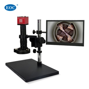
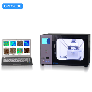
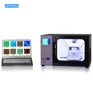
Introduction to Atom Electron Microscope
The atom electron microscope is a revolutionary instrument that provides unprecedented imaging capabilities at the atomic level. By utilizing electron waves instead of light, this sophisticated device allows researchers and scientists to visualize and analyze the minute details of various materials, making it a cornerstone in advanced materials science, nanotechnology, and biological research. Its ability to map atomic structures enables a deeper understanding of materials, paving the way for innovations in electronics, pharmaceuticals, and energy technologies.
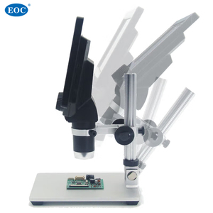
Types of Atom Electron Microscopes
Atom electron microscopes come in various types, tailored to meet specific research requirements. Here are the prominent types:
- Scanning Tunneling Microscope (STM): Offers high-resolution imaging by scanning a sharp tip very close to the surface of a conductive material, allowing for atomic-scale visualization.
- Transmission Electron Microscope (TEM): Uses transmitted electrons to create high-resolution images of thin specimens, providing insights into internal structures and defects at the atomic level.
- Scanning Electron Microscope (SEM): Provides 3D images by scanning a focused beam of electrons over the surface of a specimen, offering valuable compositional and structural information.
- Atomic Force Microscope (AFM): Measures the forces between a sharp probe and the sample surface, permitting derivative measurements like mechanical properties, topography, and more.
Applications of Atom Electron Microscope
The applications of the atom electron microscope are vast and varied, each contributing significantly across multiple fields:
- Materials Science: Used for materials characterization, helping in the development of new alloys, polymers, and nanocomposites.
- Biology: Offers detailed insights into cellular structures, virus identification, and protein complexes, enhancing our understanding of biological processes.
- Nanotechnology: Facilitates the design and development of nanostructures with precise control over atomic arrangements, which is crucial for nanofabrication.
- Electronics: Assists in the development of semiconductor materials by breaking down structures at the atomic level, leading to innovations in microelectronics.
Advantages of Atom Electron Microscopes
Utilizing an atom electron microscope presents a plethora of advantages that cater to modern research demands:
- High Resolution: Atom electron microscopes can resolve structural features at the atomic scale, enabling detailed imaging of materials.
- Versatile Imaging: Different types of electron microscopes provide various imaging capabilities, allowing researchers to choose the best method for their specific needs.
- Real-time Observation: Some advanced atom electron microscopes offer the ability to observe dynamic processes in real time, greatly benefiting kinetic studies.
- Enhanced Contrast: Electron microscopy provides finer contrast levels compared to traditional optical microscopy, making it easier to distinguish between different phases or components.